
Understanding Silicon Photonics: Link Budget and Figures of Merit

Silicon photonics is one of the hottest and fastest moving markets to address high speed data demands in co-packaged optics (CPO) in AI data centers.
In this post I’ll cover a few important high-level details of silicon photonic circuits. These include:
Link Budget
Key Figures of Merit (Laser, sources of loss, eye quality, and receiver)
Validation Challenges (wafer screening and thermal stability)
I have written on a foundational set of material from sources of truth that forms the framework this post builds upon. These include:
“A Comprehensive Overview of High Speed Optical Communications” covers a broad overview of high speed optical communications, including: conventional IMDD with pluggable optics, VCSELs, fibers, optical bands, losses, scaling challenges, integration trends including LPO and CPO, silicon photonics, external modulation, and coherent optics.

“Fundamentals of Signal Integrity” covers loss, jitter, BER, equalization and DSP techniques.

“A System Architecture Breakdown of a DSP-based Modern Wireline Transceiver” takes a look underneath the hood into a modern DSP-based transceiver, including the architectures of the DSP, ADC/DAC, and clocking circuits.

Link Budget
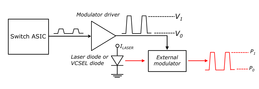
Understanding link budgeting is important to develop a system level understanding of a SiPh transceiver. Consider a typical electro-optical link with an external modulator:
At a high level, the job of a transmitter is to transmit the data at the specified data rate (224GPBS) with as low BER as possible in the given specification. Key system level performance specs include:
Power efficiency: The ratio of energy consumed to the amount of data transmitted. This is usually measured in pJ/bit.
BER: Bit error rate. Noise, loss and other effects degrade bit error rate. Requirements range between 1e-4 and 1e-6 depending on the standard.
A laser source (whether that be generated on board or coupled in externally) provides the power and is sent through a lossy modulator, connectors, and waveguides.
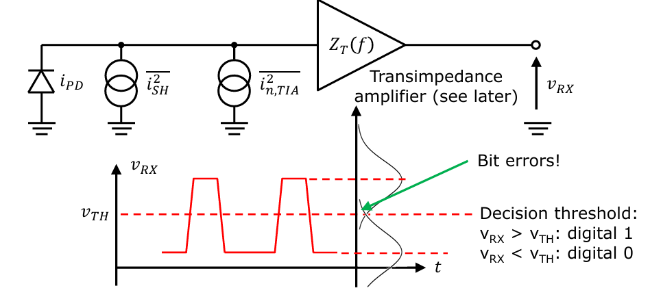
This power is then sent through the optical channel, converted back to a weak electrical signal through a photodetector, and amplified by a transimpedance amplifier. The signal at the RX need to be high enough compared to the noise in order to be able to detect the signal properly.
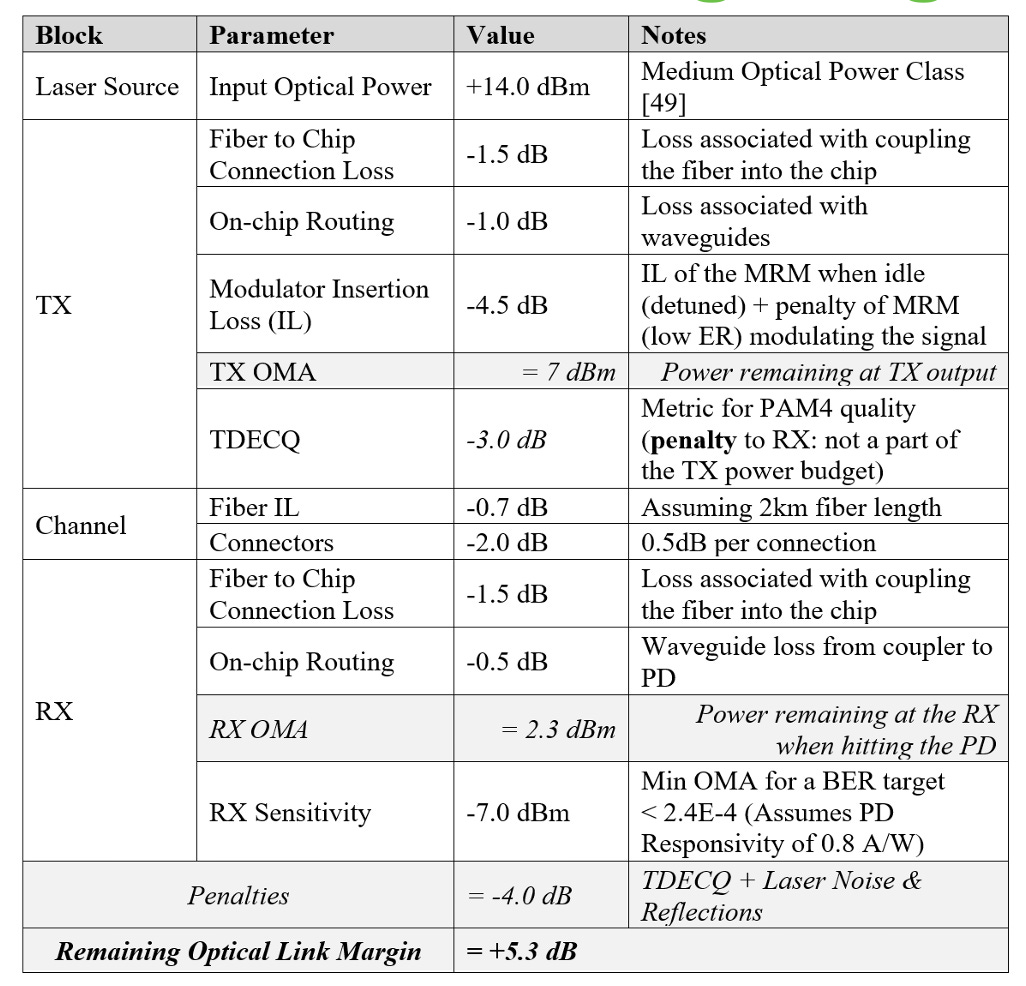
All of the sources of loss in between the TX and RX must be quantified for in a link budget in the optical chain. Lets break down each part.
Lasers
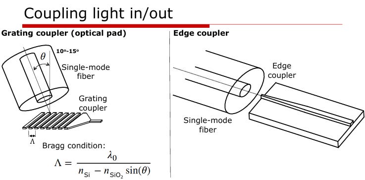
Lasers are either integrated within the PIC or coupled in externally. These external lasers are coupled into the chip through edge couplers or grating couplers.
There are a few important specifications:
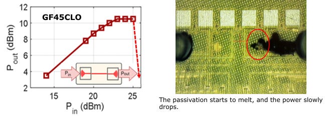
Power: The amount of coupled power is limited by two-photon absorption and other non ideal effects. Shown is a sweep of Pin vs Pout where Pout saturates and a high enough Pin can cause passivation melting:

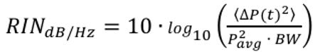
Figure 6. The Pout/Pin characteristics to couplers where the power saturations after a certain point [3] Relative intensity noise (RIN) - Rin refers to the relative intensity fluctuations of the optical signal of a laser source. This is a critically important parameter in PAM4 schemes because PAM4 has much lower noise margin than NRZ. A high RIN raises the noise floor causing a higher BER. RIN is given by:
Companies with lasers in the value chain include Lumentum, Broadcom, Coherent, Sivers, Scintil, Xscape, and Quintessent.
Losses in Connectors
There are several loss sources in the connectors themselves. These include:
Modulator loss - due to intrinsic optical absorption and scattering
Multipath Interference (MPI) - Optical reflections from multiple connectors / discontinuities
Polarization Dependent Loss (PDL) - Measures loss due to change in signal polarization
Receiver
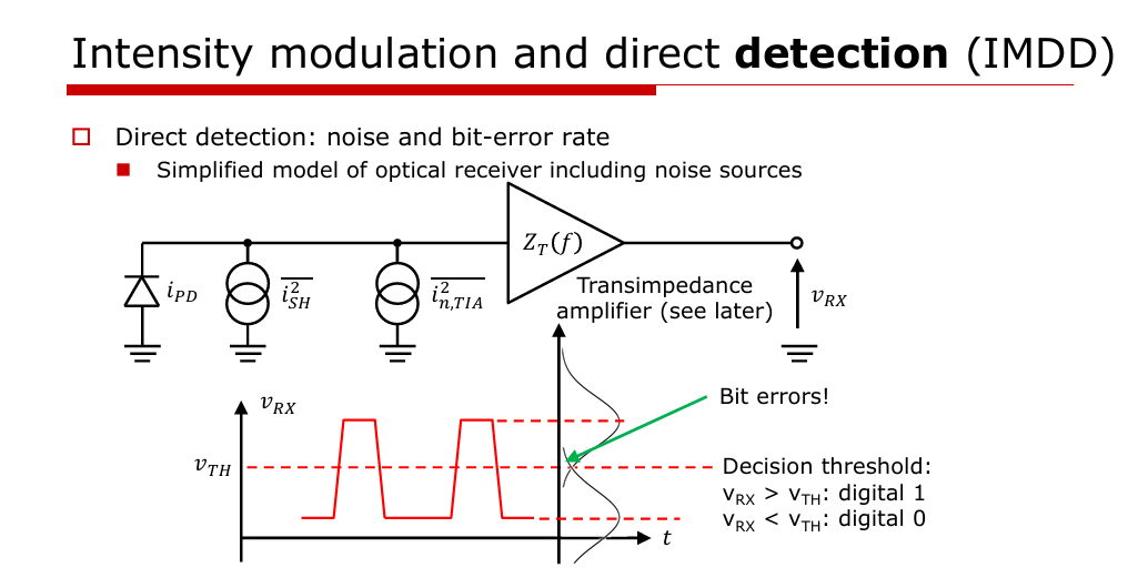
On the receive side, the signal is detected by a photodetector. This weak signal plus a noise signal is converted to a voltage through a transimpedance amplifier (TIA) that converts current to voltage.
A few key specs here are important:
Responsivity - Measures how effective the photodetector converts photons to electrons. This is typically measured in A/W.
Dark current - Measures the current flow when no light is present. Defects can cause high dark current that adds noise to RX and reduces sensitivity.
Input-referred noise - assesses the noise floor of the TIA.
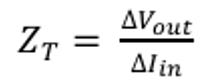
Transimpedance Gain - measures the electrical strength of the receiver. TIA gain is very important because if TIA gain is too low, output voltage swing will not be high enough to compensate for noise. It is given by:
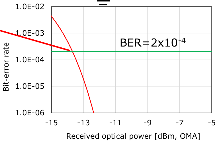
Receiver sensitivity - the minimum optical power required to achieve a specific BER target. This is determined by plotting RX BER vs OMA. BER goes down when received optical power goes up.
THD (Total Harmonic Distortion) - quantifies the non-linearity of the TIA. This affects PAM4 because it affects how even spaced out each of the four levels are after optical to electrical conversion.
Eye Quality
There are several parameters to evaluate the quality of the eye. These include:
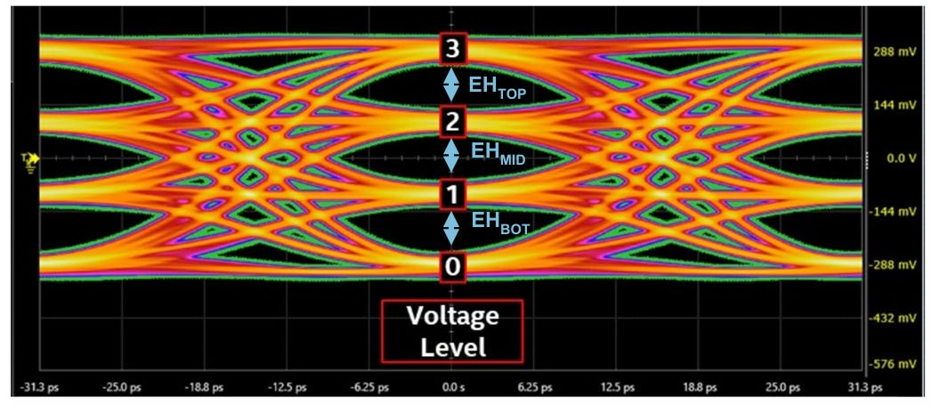
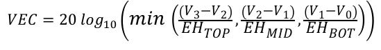
Vertical eye closure (VEC) - VEC measures the quality of the electrical signal going through the electrical channel before entering the optical module. VEC calculates the smallest eye height of all three eyes and is given by:
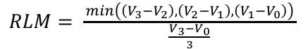
Ratio of Level Mismatch (RLM) - measures the vertical symmetry of the three eyes. It is given by:

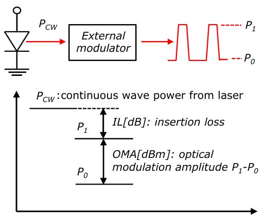
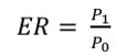
Extinction Ratio (ER) - measures the power ratio between levels. This is given by:

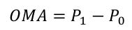
Optical Modulation Amplitude (OMA) - Measures the modulation swing “strength” as the power difference:

Side Mode Suppression Ratio (SMSR) - Assesses optical crosstalk, which is especially relevant when using several optical wavelength for aggregated data transmission
Transmitter and Dispersion Eye Closure Quaternary (TDECQ) - This measures the eye closure / power penalty required to compensate for any imperfections of the TX. This is given by:
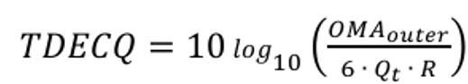
This needs to be lower than 3.4dB for a successful link by IEEE standards.

Challenges with Validation of SiPh
Validating SiPh suffers from a few key challenges:
Wafer level testing
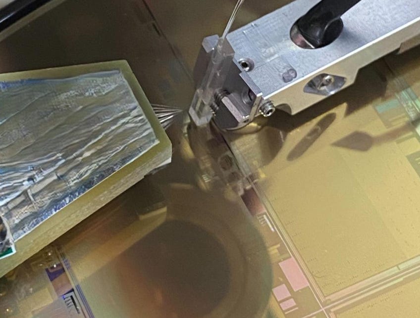
One key challenge of SiPh is screening of wafers. When SiPh devices are designed for edge coupling, light can’t be coupled with the wafer intact during wafer-level testing. Instead, grating couplers are used in place to externally apply a laser source. These grating couplers do add a higher IL that needs to be calibrated out with embedded calibration structures.
Temperature stability
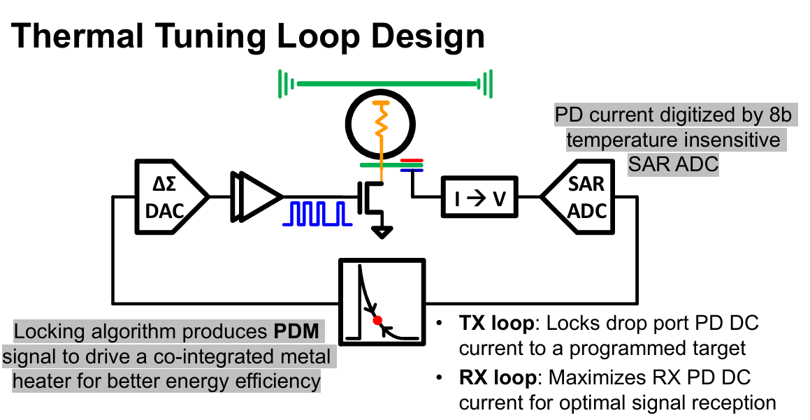
Modulators are inherently sensitive to temperature fluctuations that can shift wavelengths. Ring modulators are particularly sensitive, especially in compact DWDM architectures with many rings cascaded in close proximity where heat generated from one ring can influence the others. Thermal tuning loops are put in place to help stabilization the temperature of the modulator, like the one shown by NVIDIA.
Conclusion
There are many effects that impact the quality of signal integrity and contribute to loss that must be accounted for. SiPh solutions must evaluate sources of loss and noise across the chain to determine the most optical solution for the given application.
If you learned something of value from this post, please share / restack this post so that others may benefit from the knowledge as well.
References
[1] Ossieur, P. “Introduction to Optical Communication Systems From VCSELs, integrated photonics to coherent solutions” ISSCC 2026
[2] Nourzad, M and Liu, Y. (Lightmatter) “Navigating the New Frontier: A Guide to Testing Silicon Photonics High-Speed Links” DesignCon 2026
[3] Aflatouni, F. “Silicon photonics-based solutions: components, circuits, and integration” ISSCC 2026
[4] Song, S, et al (NVIDIA) “A 32Gb/s/λ 256Gb/s/Fiber Half-Rate Bandpass-Filtered Clock-Forwarding DWDM Optical Link in a 3D-Stacked 7nm EIC/65nm PIC Technology” ISSCC 2026