
A Comprehensive Overview of High-Speed Optical Communications
Scaling high-speed data movement from IM-DD to Copackaged Optics/Coherent/Silicon Photonics

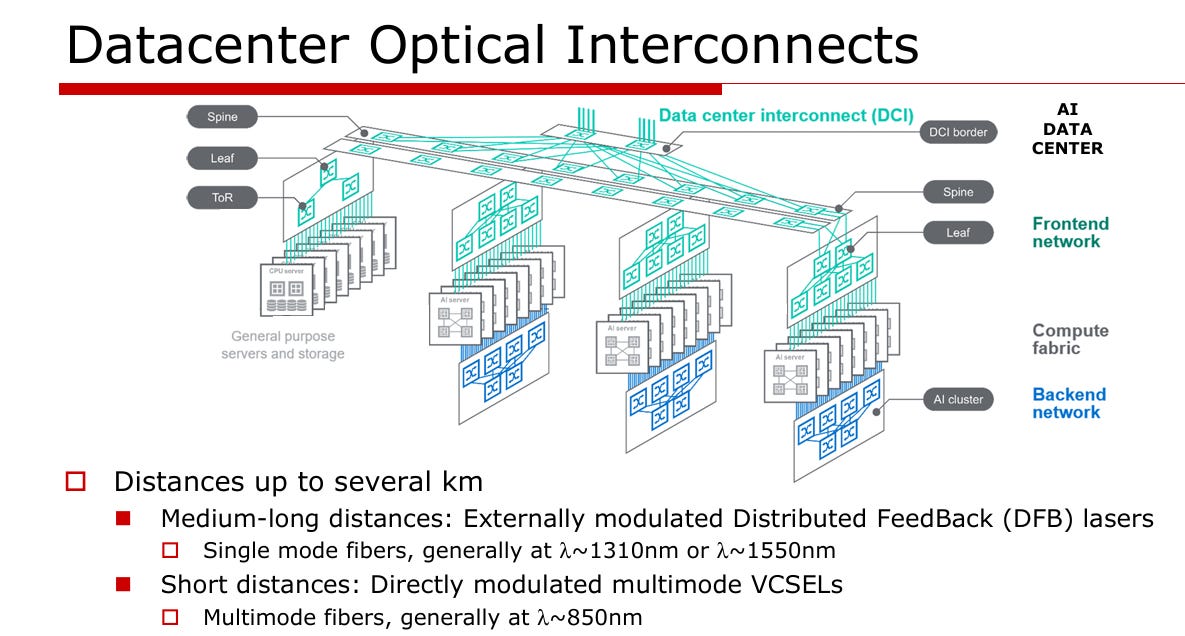
High speed optical interconnects have become one of the hottest markets in AI data centers. As bandwidth demand rises, the challenge is no longer just computing on data faster, but moving it across packages, boards, racks, and clusters efficiently.
The optical space has exploded over the past few years with many companies and startups proposing solutions to tackle data demands.
But I want to step back and ask ourselves: what are the first principles challenges with scaling high-speed optical communications?
In this post I will cover entire optical communications space:
I will introduce the conventional IM-DD optical approach with VCSELs used for short reach
I will then highlight challenges with scaling conventional IM-DD to higher data rates
Then I’ll explain techniques to improve data bandwidth:
Co-packaged optics
Silicon photonics
External modulation
Coherent optics
I worked up to this post by first writing primers on the architecture of a Modern SerDes Transciever and selected subsystems & interfaces (PLL, SAR ADCs, Bandgaps, and Signal Integrity). I aim to keep these high level as possible without delving into too many details. These posts, along with this one, form the core of high-speed data communications in AI racks at a first principles, systems-thinking level.


My goal with writing these is to provide a “mental model” to help you understand the system context and trends in the optical communication space better, no matter what part of the stack you are working in. I’d recommend giving these a read because I will reference concepts and tradeoffs here that I described in full detail in those posts.
The workhorse for short reach - IM-DD & Pluggable Optical transceiver
The workhorse for short reach optical communications today are IM-DD with pluggable optical transceivers. Lets take a looks at what each consists of.
Intensity Modulation - Direct Detection
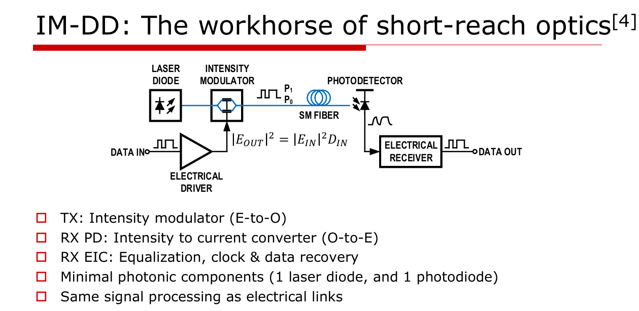
IM-DD is the workhorse of short reach optics. IM-DD encodes information in optical intensity (whether that be 0/1 or higher levels in PAM4) and recovers it through direct detection.
This intensity modulation can be performed in one of two ways:
Direct modulation - the laser is turned up/down by the electrical signal
External modulation - a driver modulates a steady optical carrier
Pluggable Optical Transceivers
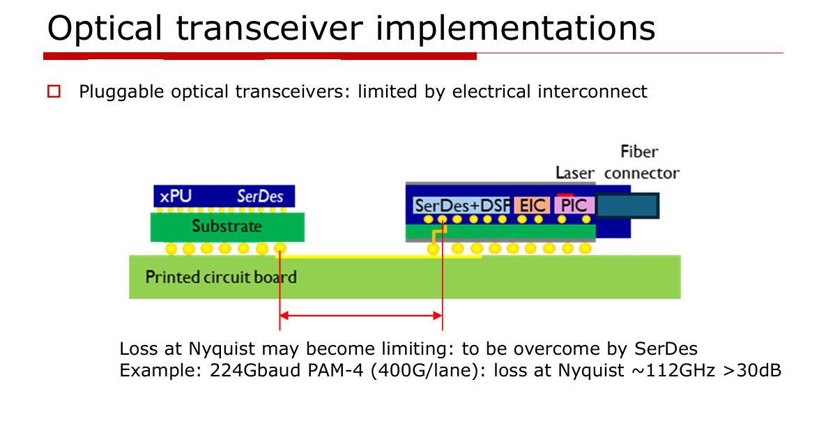
These IM-DD are typically packaged into pluggable optical transceiver modules that sit far away from the chip. These are are match-box sized modules that take in electrical (client) side data and convert it to optical (line side). Each block consists of following:
Serdes + DSP - For serializing / desterilizing the data from/to host and perform equalization
EIC - Electrical integrated circuit - consists of the electrical circuits fabricated in electrical processes (drivers, mixed signal conditioning, etc)
PIC - Photonic integrated Circuit - consists of the optical circuits fabricated in optical processes (Si Photonics, VCSELs, etc)
Optical transceiver modules are a very mature technology that has scaled in data throughput for many years. However, with AI workloads demanding 224+ GPBS throughput capability, the performance of the optical transceiver itself needs to adapt, as well as the signal integrity between host die and optical engine.
System architecture breakdown of a IM-DD
Next I will break down the architecture of an IM-DD in each of its components:
Transmitter
Fiber
Receiver
I will discuss several options for each and important design considerations.
TX Driver - Direct Modulation
Laser (Light amplification by stimulated emission of radiation)
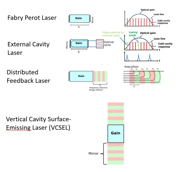
Lasers are powered by a large pump current stimulating emission. Photons with energy close to the material bandgap interact with electron - hole pairs and cause identical photons to be emitted. This causes an “optical gain” of photons within the active region.
This photons is then confined using two mirrors: one opaque, and other that is semitransparent to allow the light to shine through.
Lasing occurs when the pump current is high enough such that optical gain > optical losses.
Then, either a cavity structure or frequency selective bragg reflectors selects which optical modes are sustained.
In a Distributed Feedback laser (DFB) laser, a periodic grating of Bragg reflectors provides wavelength - selective optical feedback, favoring a narrow lasing wavelength. These Bragg Reflectors are highly tunable depending on the index of refractions and the lengths and # of sections.
VCSEL (Vertical-Cavity Surface-Emitting Laser)
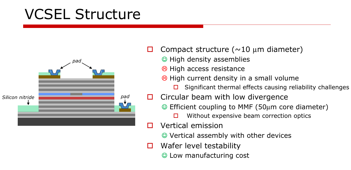
VCSELS are lasers that emit light vertically in a circular cross section. The active region consists of multiple quantum wells that enhances optical gain. Distributed bragg reflectors are stacked on the top and bottom of the active region with alternating refractive indexes. These layers are fabricated using epitaxial growth on a substrate.
The light is then confined with an oxide and current is pumped in through pads. The light is shown vertically above and redirected toward the optical fiber with optics.
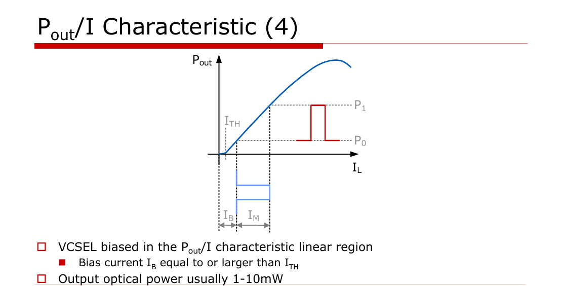
The Pout/I of VCSELs almost resembles a linear diode. The VCSEL begins lasing above a particular threshold current and exhibit a linear relationship between Pout / Iin over a useful operating region. Lasers require a DC bias to set the device in the linear region.
One important parameter is the extinction ratio, which is the ratio between P1 and P0. A higher extinction ratio is preferred as it improves BER margin to detect teh signal at the other end, but higher extinction ratios require higher currents, and therefore power, to drive the device.
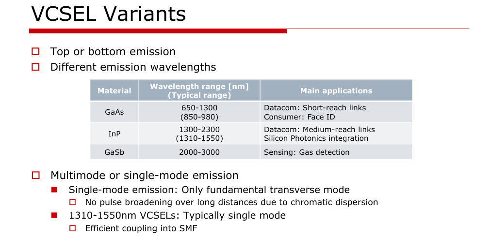
The two major materials used in lasers are GaAs or InP:
850 nm GaAs VCSELs are common for short-reach multimode links.
1310/1550 nm InP-based lasers/modulators are common where single-mode fiber, longer reach, or telecom/datacom bands matter.
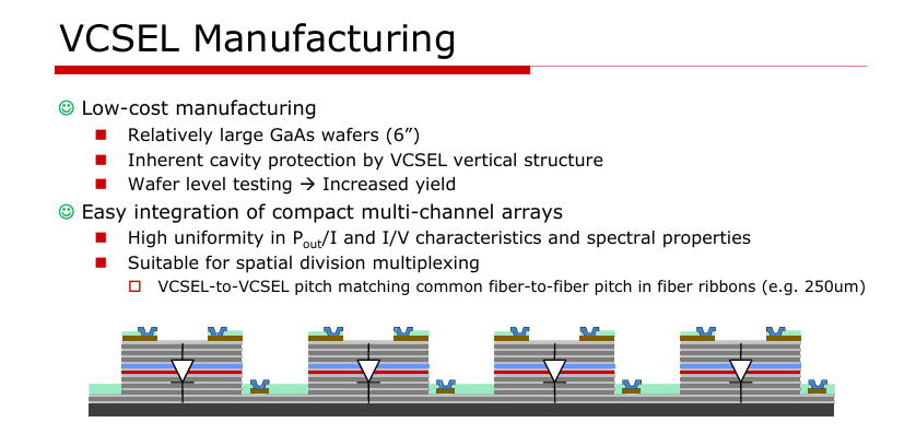
VCSELs are very popular in short reach communications for a numbers of reasons:
Low cost manufacturability - they are easy to test on-wafer across multiple samples
Scalability - they can be formed in “arrays” to drive multiple optical lanes
However, VCSELs do have some drawbacks:
Reliability - issues due to oxide confinement and high currents degradating mean-time-to-failure
Signal switching nonidealities, including:
Turn on delay- a delay in the turn on of the signal that adds to latency
Jitter - uncertainty in the signal edge that degrades BER
Relaxation oscillation - an “underdamped” response in the turn-on characteristic that can affect BER and signal quality
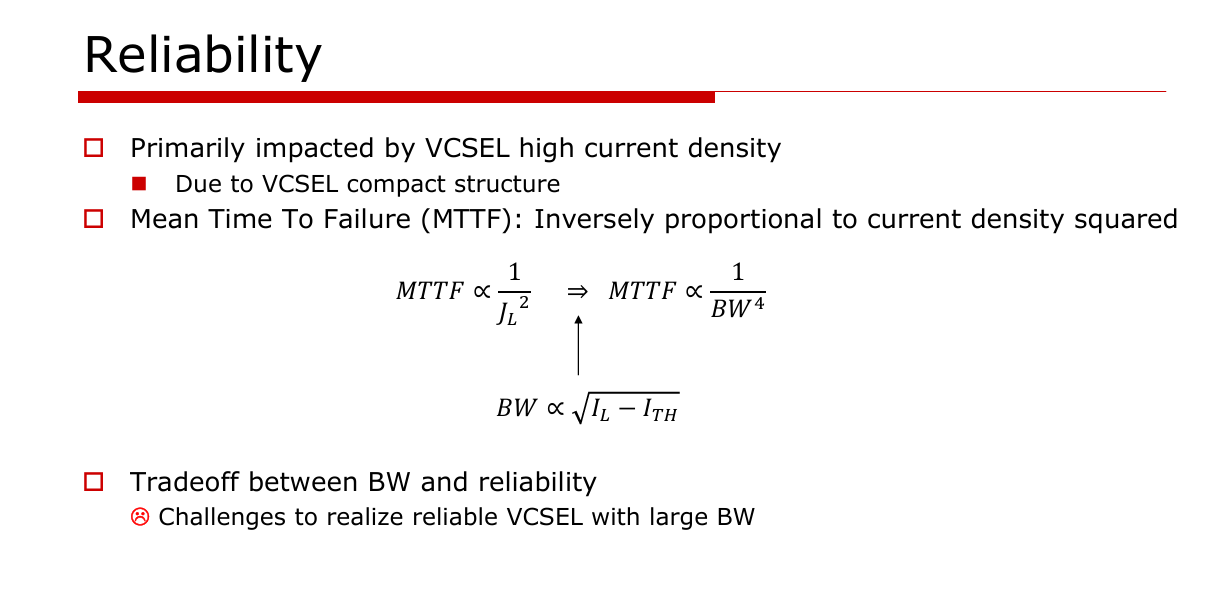
The main tradeoff in VCSELs is between BW and reliability. Higher current densities allow for higher BWs, but it also decreases the mean time to failure, a common metric used when evaluating reliability.
Driving the Laser
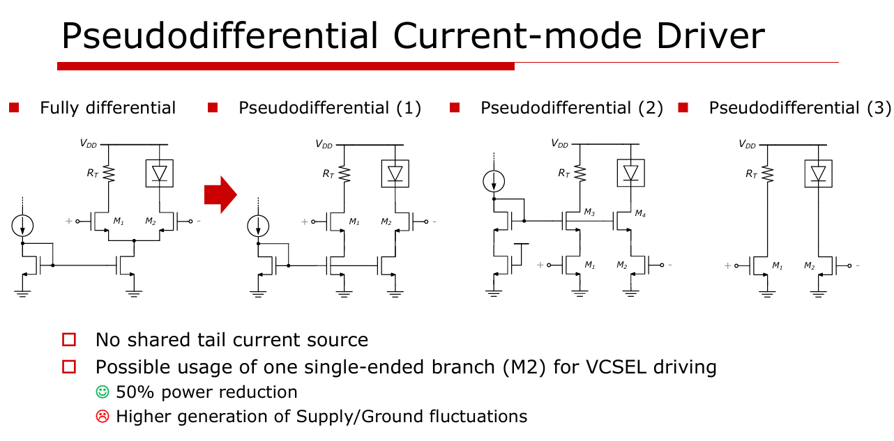
Here are a few DC coupled, common anode circuits used to to drive the laser directly using either fully differential or pseudodifferential to convert a voltage to a current to drive the VCSEL. There are other methods of driving such as common-cathode, BJTs, and push-pull implementations depending on the requirements of the system.
In general, the more VCSEL current that is needed, the slower the driver will be due to increasing output capacitance.
Fibers
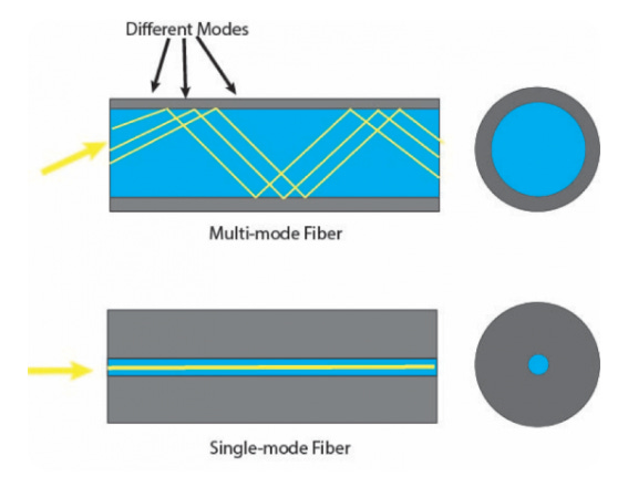
Multimode fiber optic cables are primarily constructed from silica glass (silicon dioxide). There are two major categories of fiber for high speed communications:
Multimode - Uses a larger core (50–62.5 um) to transmit multiple light paths
There are five classifications, OM1-5, that grade the quality of the fiber.
Pros: Cost-effective for short-distance, high-speed applications
Cons: Limited distance due to higher signal modal dispersion
Single Mode - Uses a smaller core (8-10um) to transmit a single mode of light
Pros: Low signal loss, avoids modal dispersion
Cons: Higher cost of laser components and more complex installation requirements
Generally speaking, multi-mode fibers are used for short reach interconnect due to its low cost and complexity. However, single mode fiber is being evaluated to “future proof” the data communications since it can support the higher BWs, though it adds to cost and integration complexity.
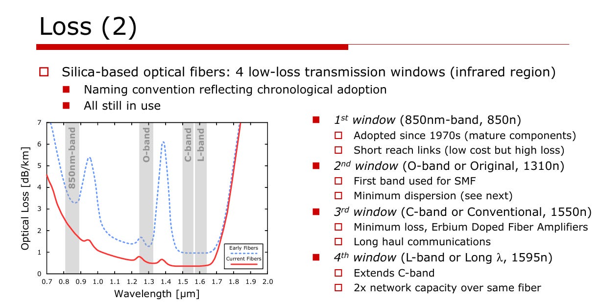
There are also four wavelength bands used in the fiber:
850nm band - used for short reach links
O-Band - 1310nm
C-band - 1550nm
L-Band - Extends C band to allow 2x network capacity
There are four major impairments:
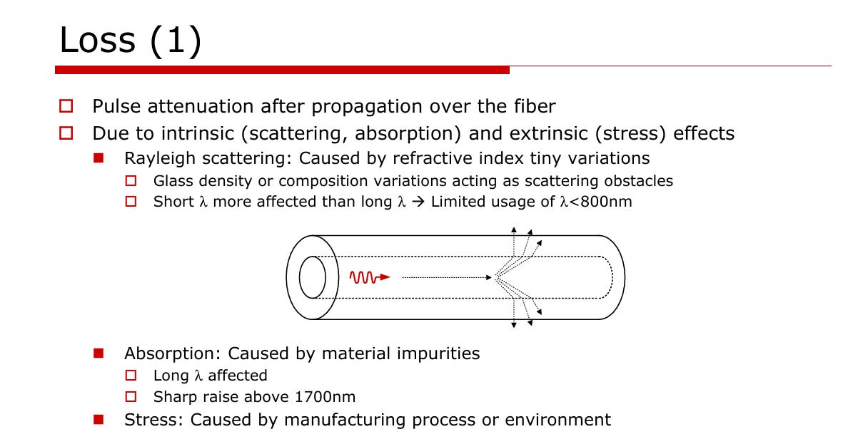
Loss. Losses cause pulse attenuation after propagation from a fiber. These are caused by intrinsic sources, including
Rayleigh Scattering
Absorption
Manufacturing Stress
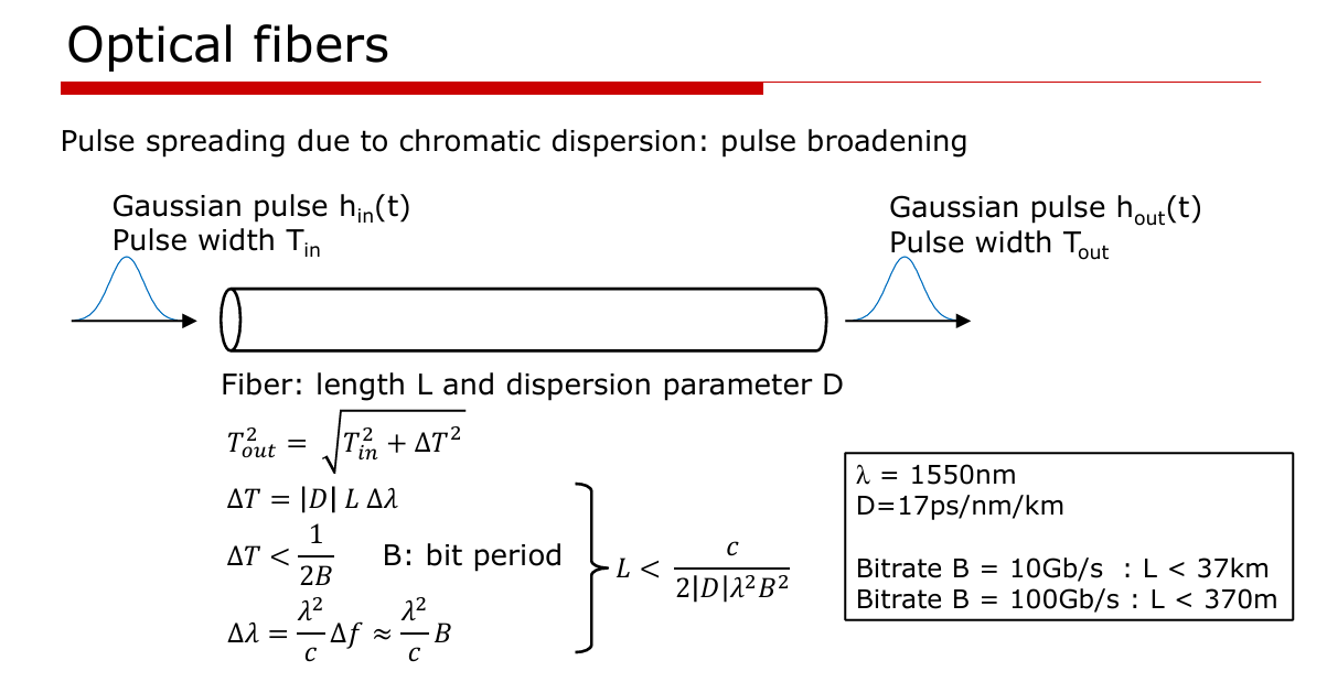
Chromatic Dispersion - pulse spreading after propagation over the fiber. This is caused by fiber refractive index dependence on wavelength
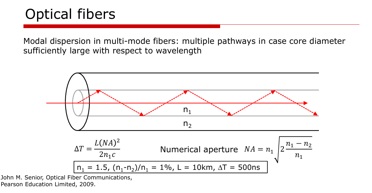
Modal dispersion - distortion due to different propagation delays of different optical modes. Modal dispersion matters in multimode fiber.
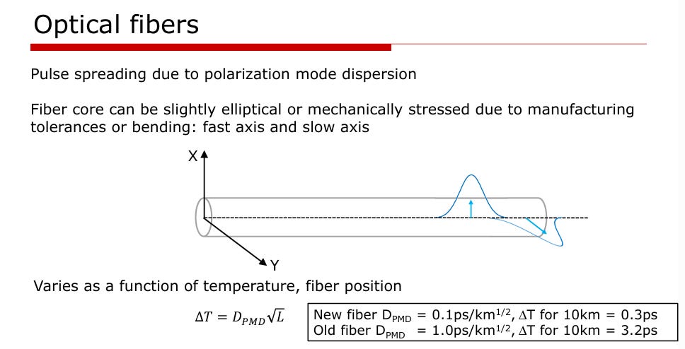
Figure 15. Polarization Mode dispersion in optical fibers [3] Polarization Mode dispersion (PMD) - dispersion cause by pulse spreading of different polarizations due to asymmetries in the fiber core.

Receiver - Photodetector
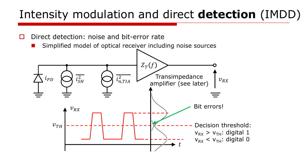
A photodetector consists of a Reverse biased PIN junction that generates current proportional to the detected light. The transimpedance amplifier then amplifies this current to an output voltage at the other end.
There are some important specs of this system:
PIN characteristics: Responsivity, capacitance, noise, dark current
Receiver Q-factor: The received signal level relative to total receiver noise
BER: BER can be derived from this Q factor: BER = 1/2*erfc(Q/sqrt(2))
A higher extinction ratio is desired to ease the burden on the receiver, but it does come with a higher power usage.
Why Scaling IM-DD is hard
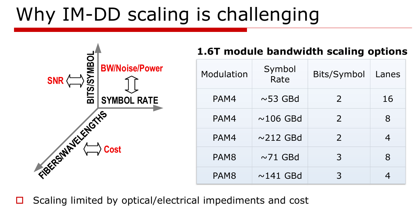
Scaling IM-DD to higher data throughputs is hard due to several unfavorable tradeoffs between BW, reach, noise, power, SNR, and cost. These include effects in both optical and electrical domain themselves:
Optical
Chromatic dispersion
Polarization Mode dispersion (PMD)
Nonlinear and interference effects
Electrical
Noise penalties at Higher BW
Tighter jitter, skew, and ISI
BW scaling limits in front ends
You can have the fastest optical transceiver, fiber, but its pointless if the signal can’t get to it fast enough. Not only the optical receiver itself needs to improve, but the signal integrity from the electrical interconnect is running into challenges shuttling high speed data back and forth. Solutions need to ensure that speed “bottlenecks” within the system scale with the system demands.
This leads to four major trends that generally increase complexity:
Co-packaged optics - embedding optical components within the package itself
Silicon Photonics - routing light through silicon waveguides and modulating it
External modulation - modulating a continuously running laser for higher BW
Coherent Optics - modulation amplitude and phase in the optical domain
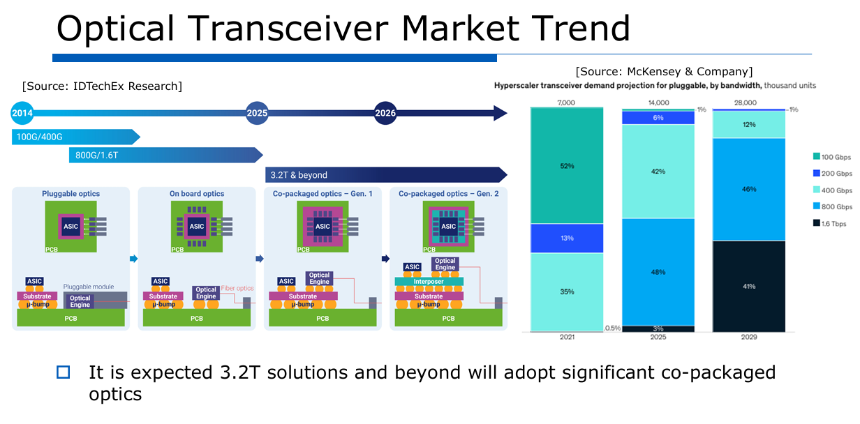
Integration Challenges: Co-Packaged Optics
Co-packaged optics is one solution as part of a broader effort to tightly integrate the optical module and the host chip to reduce SI challenges at high speeds.
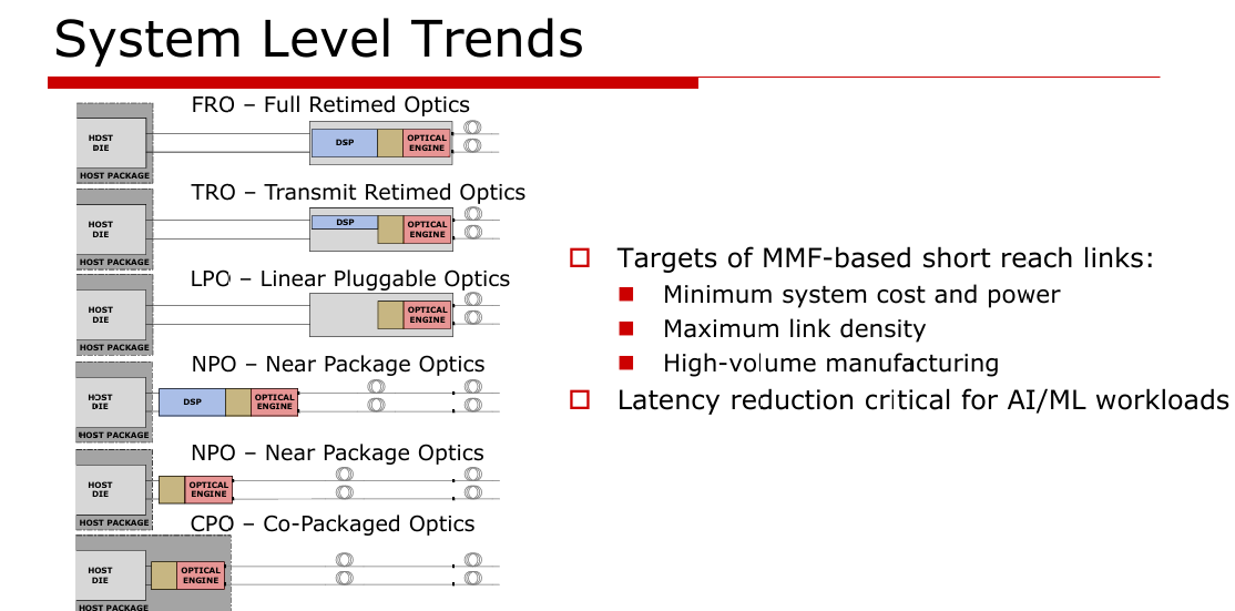
Transitioning from module-based optics to integrated optics involves two things:
Shortening the distance between host die and optical engine
Shifting the processing complexity to the host die
In the progression from FRO to TOP and PLO, the DSP burden is shifted into the host die itself. This DSP performs necessary functions such as equalization and error correction. Since the SerDes is further away from the optical engine, this requires co-design along with the transmission line to ensure proper performance.
Then, in NPO, the optical components themselves are custom placed close to the package. This shortens the distance between the host die and the optics itself and enabled greater speed scaling. However, it does require much tighter integration within the system.
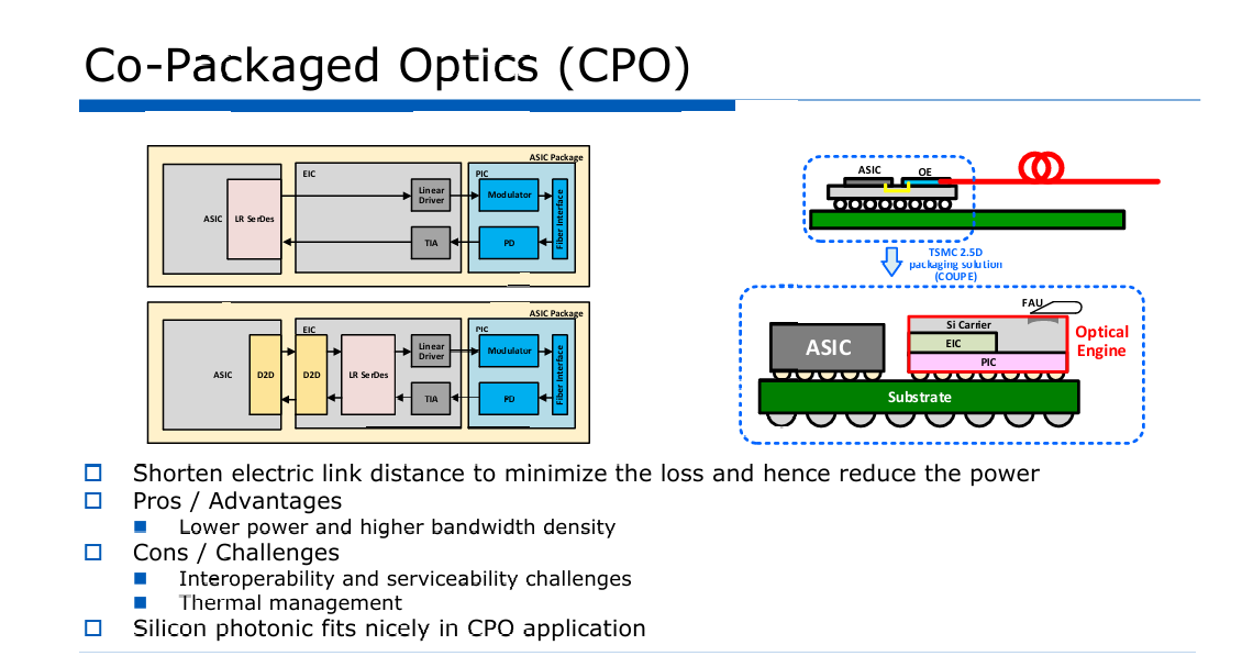
The most optimal performance solution is co-packaged optics, which mounts the optical engine on the host die package. This has many benefits, but the main issues are thermals closer to the ASIC, reliability, more complex upgrades, and less mature technology. Remember, components can and do fail in data centers and need to be replaced, which can cost the data center money.
The developments around co-packaged optics is messy because different companies are optimizing for particular aspects of the optical value chain.
Silicon Photonics
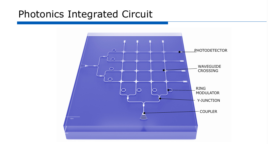
On the die itself, silicon photonics enables better integration with silicon processes. In a systems, an electronic integrated circuit (EIC) is stacked vertically on top of a photonic integrated Circuit (PIC) that handles the lasing and signal conditioning in the optical domain.
Compared to mixed-signal circuits, silicon photonics circuits have less devices, but the devices themselves are heavily based on solid-state physics and have material properties that must be taken into account in the design process.
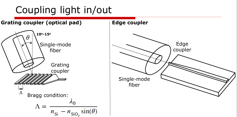
Many practical silicon-photonic platforms rely on heterogeneous integration or external lasers for active optical functions because silicon itself is not an efficient light source or optical gain medium. In the PIC, light can be coupled into one of two ways:
Grating Coupler - vertical coupler where light is shown into a Bragg reflector
Pros: Easy, flexible, wafer scale testing
Cons: Low efficiency, narrow BW
Edge Coupler - coupling in light from a single mode fiber to a tapered SiPh line
Pros: High efficiency, broad BW, lower polarization
Cons: Required precise facet polishing dicing and less flexible placement
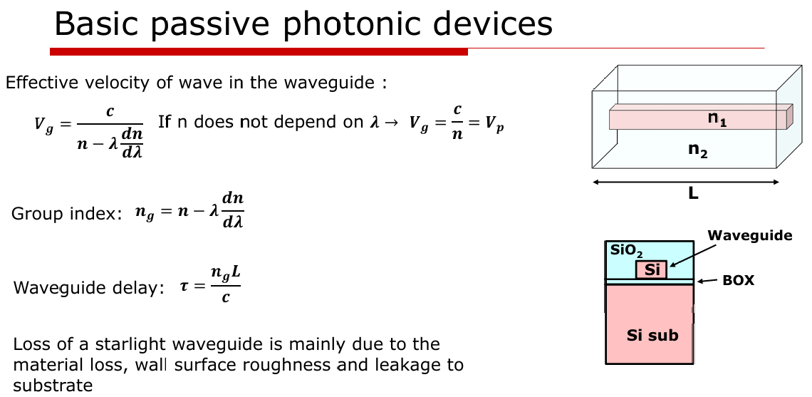
This light is then passed through silicon waveguides that is then operating in a few different “modes”. The waveguide itself has a index of refraction n1 and the oxide has another index of refraction n2. For confinement to occur, n1>n2. In silicon photonics, n1 ~ 3.48 and n2 ~ 1.5.
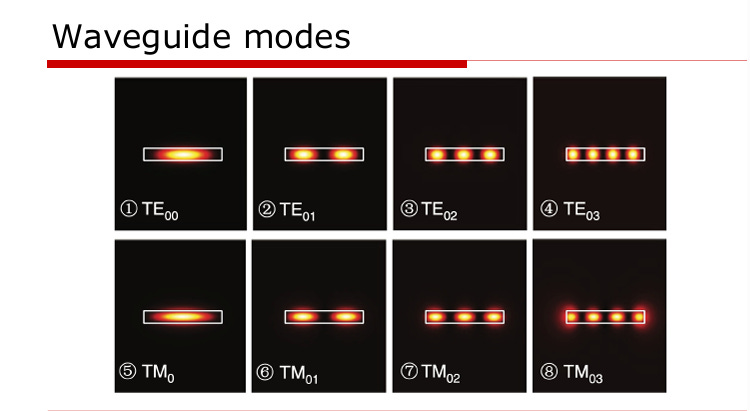
This light then operates in different modes depending on the width of the line itself. It can operate in either single mode or multimode. Then, this light is then modulated externally through one of several external modulators I will discuss in the next section.
SiPh is a very promising technical area enabling much better integration anf faster speeds, but it presents several challenges:
The amount of power you can couple into the chip is limited due to two-photon absorption.
Surface roughness increases loss. Optical signals that come closer to the surface in higher-order modes exhibit greater loss.
Bends in the waveguide are not trivial since they can excite undesired modes and cause additional loss.
Optical signals have a power overhead - Optical interconnects must provide a lower power solution to replace copper
The holy grail of silicon photonics is silicon optical amplifiers and lasers that can be fabricated on standard CMOS processes.
External Modulation
Silicon photonics typically employs external modulation. As opposed to direct modulation which turns the laser source on/off, external modulation is used to “blank” a continuously running laser. There are three major categories of external modulation: Mach-Zehnder, Electro-absorption, and ring modulation.
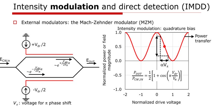
Mach-Zehnder Modulators is a very commonly used external modulator due to relative simplicity in layout and modelling. MZM operate by modulating the phase of an optical signal split into two branches. This voltage is typically driven differentially to ensure symmetry in between the branches. Then the signals are recombined at the output.
The output can either constructively or destructively interfere. This phase shifting operate causes an oscillation pattern in the normalized field output vs drive voltage. The device can be biased around a center point and thus modulated to control the signal sent through.
MZMs can be implemented in either Silicon Photonics, InP, or Hybrid Silicon - LiNbO3.
MZMs are fairly straightforward in principle, but present a few challenges:
The area is quite large to ensure that enough “phase” of each signal accumulated
At high frequencies, the lines must be treated as transmission lines and so the voltage sent down the line must be faster than the speed of the optical signal. Depending on the speed, the voltage signal may need to be “repeated” in different sections along the line.
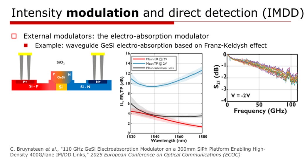
Electro-absorption modulator - These are modulators that act like direct “switches”. They consist of PIN diodes that are embedded within the waveguide the optical signal goes through. The idea is that the PIN diode bandgap moves with applied voltage and affects the optical absorption.
These modulators can be extremely fast (100GHz)
However they are fairly nonlinear, making it difficult for schemes like PAM4
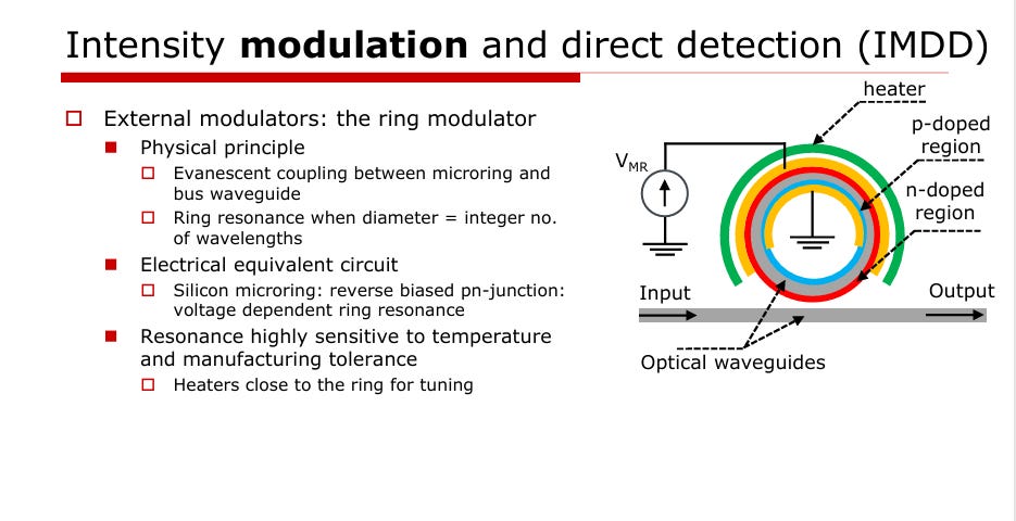
Ring Modulator - the idea is that a micro-ring is placed next to a bus waveguide with evanescent coupling in between. The signal resonates inside of the ring when the diameter equals the integer number of wavelengths.
Ring modulators are very small
Rings can support many resonances, making it convenient for wavelength multiplexing
However, the resonance is highly sensitive to temperature and manufacturing tolerances. As a result, heaters are placed close to the ring for tuning.
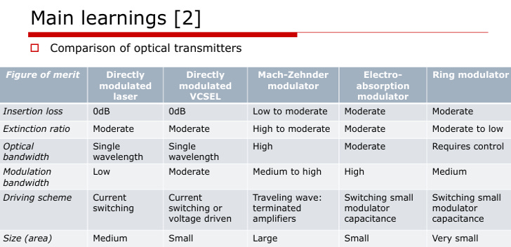
A comparison of all of these modulator schemes is shown in the above table. As you can see, external modulators tend to have much higher modulation and optical bandwidths, but impose insertion loss and size penalties in some cases.
Coherent Optical
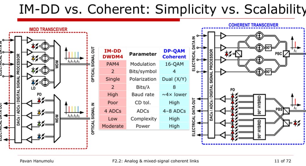
This brings us to the last topic, Coherent Optical, that I’ll briefly cover. Coherent optical transceivers encodes both amplitude and phase in the optical field, often with two polarizations, and recovers it using a local oscillator and DSP.
A common coherent transmitter uses nested Mach–Zehnder modulators to generate I and Q components. More advanced transmitters may duplicate this structure across two orthogonal polarizations for dual-polarization coherent signaling.
Coherent optical is already dominant in long haul, underseas cable data rate environments. It is being actively explored for short haul, high BW links that can “future proof” future optical designs.
However, coherent adds additional complexity, power and tighter integration challenges with co-packaged optics.
Conclusion
This post covered the broad foundations of optical to help you better understand trends in the optical space a lot better. Co-packaged and coherent optics are very promising ways to scale high speed data communications in the near future.
If you enjoyed this, please subscribe so you don’t miss out on the latest.
Also make sure to check out my other posts and share posts with colleagues you feel might benefit from this information to help them understand how their part plays a role in the entire system.
References
[1] Temporiti, E. “VCSEL-based Solutions: Components, Circuits and Integration” ISSCC
[2] Hanumolu, P. “Analog and Mixed-Signal Approaches for Low-Complexity Coherent Optical Links“ ISSCC
[3] Ossieur, P. “Introduction to Optical Communication Systems From VCSELs, integrated photonics to coherent solutions” ISSCC
[4] Aflatouni, F. “Silicon photonics-based solutions: components, circuits, and integration” ISSCC
[5] https://blogs.cisco.com/sp/fiberopticspt2singlemultifiber
[6] Chen, E. “State-of-the-Art 200+ Gb/s Electrical and Optical Interconnects” ISSCC
[7] Jain, R. “Scaling AI with Light: 3D Photonic Solutions for Next-Gen Connectivity” ISSCC
[8] Hossain, M. “Electrical and Optical Links Towards 400G+ Connectivity” ISSCC