
The SAR ADC: A Primer
How SAR ADCs operate at the interface of signal, power, digital logic, and timing

ADCs are the toll booth amongst multiple “worlds” on the chip. When a signal gets converted from one world to another, a “tax” is paid in the form of power consumption, latency, or accuracy.
Successive Approximation Register ADCs (SAR ADCs) are widely used due to their amazing versatility. They can be optimized for speed, resolution, or both due to the ability to scale the architecture in the analog and/or digital domains.
SAR ADCs have seen great use especially as process nodes allows complexity to be abstracted in digital. They are used in a variety of applications:
RF / Wireline transceivers
Sensing (Touch, Biomedical)
Analog Compute-in-Memory
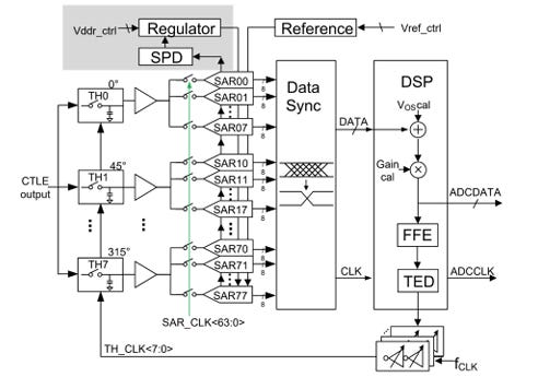
In a real system, such as a modern wireline transceiver, ADCs often interact with other blocks such as PLLs to generate the clocks, LDOs to power the circuit, bandgaps to generate the references, and DSP to do digital post processing. Additionally, SAR ADC can be time interleaved to increase data throughput.
Basic Architecture of a SAR ADC
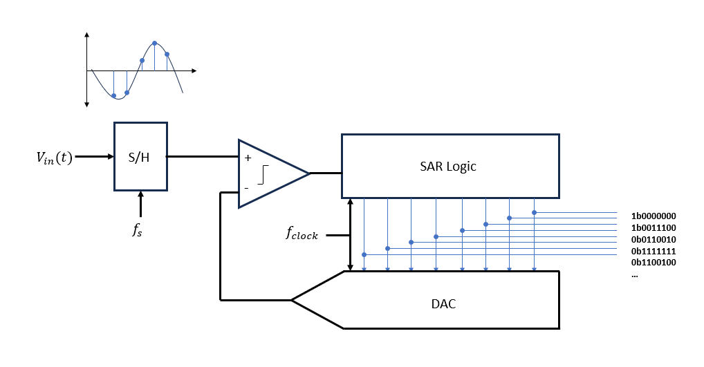
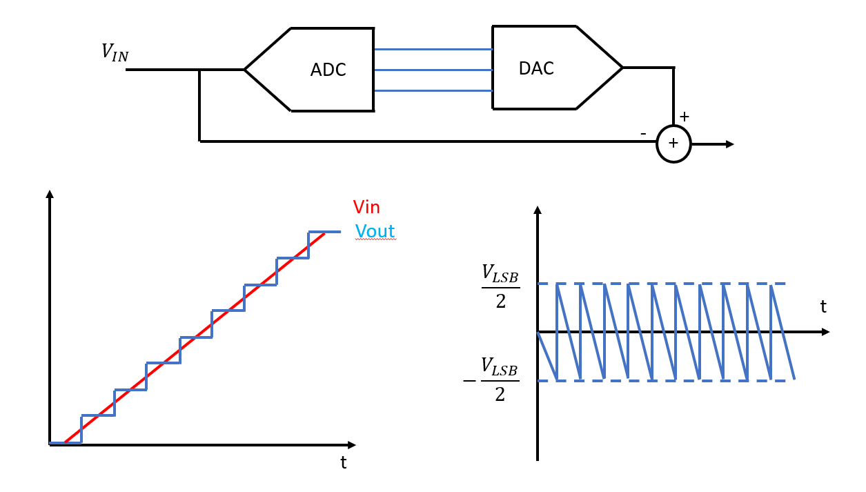
SAR ADCs use a DAC in a feedback loop that compares the input against digital code. The digital codes are adjusted until the error is minimized in the comparator.
A SAR ADC comprises of the following building blocks:
Sample and Hold. This circuit samples the signal at a sampling frequency fs and holds it in place for conversion
Comparator. A comparator compares the input reference to the DAC output and tells the SAR logic whether to increase or decrease the voltage
SAR Logic. A digital block that implements a “binary search algorithm” by cycling through digital bits in response to the voltage error
DAC. This block converts the digital code into an analog value to be compared against the input reference
SAR ADCs have the following output transfer function that resembles a “stairstep”:
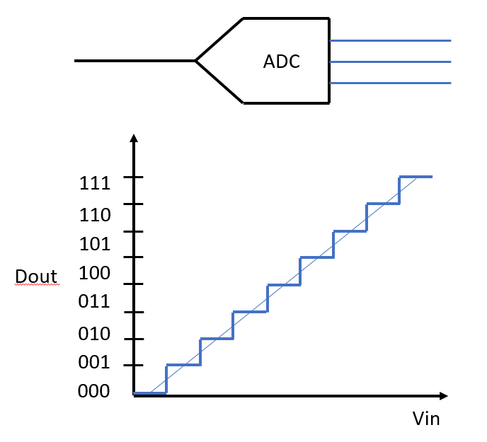
This is the ideal behavior, but SARs ADCs are very sensitive to matching, noise, and non-ideal components that cause the output to deviate from this ideal stairstep. These effects are especially pronounced in the DAC. Good layout techniques as well as calibration can be used to compensate for the errors. More on that later.
The Binary Search Algorithm
SAR ADCs use the “binary search algorithm” in order to figure out the right digital code that minimizes the error between the voltage input and the DAC output.
Binary search is an algorithm that is widely used in SW for storing values in a “tree” structure with left nodes for lower values and right nodes for higher values. In the context of SAR ADCs, the basic idea is that:
If your DAC voltage is higher than the reference, adjust the digital bits to make Vout lower
If your DAC voltage is lower than the reference, adjust the digital bits to make Vout higher
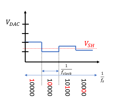
This process takes place from coarse resolution to fine resolution. That is, you make your biggest voltage changes first, then you make smaller voltage changes as you narrow in on the closest digital value.
To complete an N bit conversion, N clock cycles are usually required. For this reason, there is a fundamental tradeoff between speed and resolution since it will take longer for the circuit to converge on a higher resolution value.
Charge Redistribution DAC
This SAR logic feeds into a DAC, which is most commonly implemented as a charge redistribution DAC. Shown is a fundamental architecture that explains the behavior, and served as the foundation of understanding more modern implementations. [1]
Here, the capacitors are binary weighted. There are three phases of operation:
Sampling phase: Sample the input onto the capacitor array
Hold Mode: Disconnect the input and establish the initial comparator condition
Bit Cycling: Successively switch capacitor elements between reference levels to test each bit decision
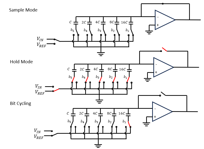
In some implementations, the capacitor array is switched between a + and - Vref voltage. In other implementations, Vin is directly connected to the top plate of the capacitor array that is switched off during conversion
One major source of error in binary DACs is capacitor mismatch, which can get bad as capacitor sizes get exponentially larger with increasing bits with binary code. The mismatch caused by capacitor ratio errors can cause errors in your codes that makes your effective resolution much lower than what your DAC architecture supports.
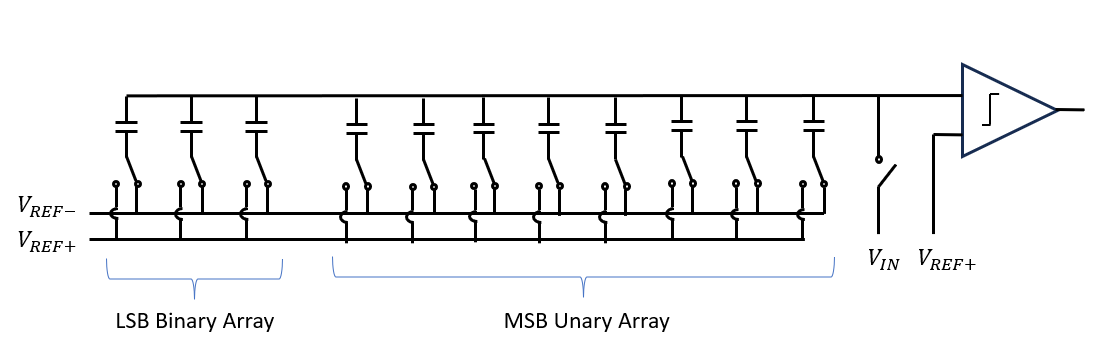
To get around this, a technique called “segmentation” is used.
Segmented DAC
Segmented DACs allows ADCs to be “customized” by blending different architecture for the MSBs and LSBs. Segmented DACs split the architecture in two “halves”:
LSBs are Binary Code: Encode each value through a binary weighted sum of DACs
MSBs are Unary / Thermometer code: Encode the MSBs using unary code which uses unit sized capacitor values. These capacitors tend to be “arrayed” in 2D especially as resolution increases.
Segmenting allows much reasonable component sizes and ratios in the binary side and better matching of unit sized capacitors in the unary side. Typically the unit sized capacitors are implemented as a 2D array on chip that can be switched to any size needed. However, this added area does introduce other sources of error due to trace parasitics that should be accounted for.
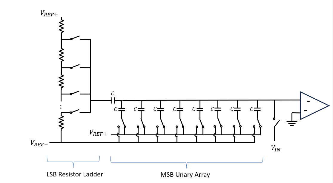
Another common implementation is using a resistor ladder for the LSBs:
Charge Redistribution DACs allow for low power as the conversion is being done through finite amounts of charge moved around. There are other DAC architecture such as current-steering that optimize for speed at the cost of the power consumed from continuously flowing currents.
Important Specifications
There are several specifications to ADCs.
Resolution. Resolution refers to the number of distinct analog level that correspond to the different digital words. A 10 bit resolution corresponds to 2^10 or 1024 distinct analog levels.
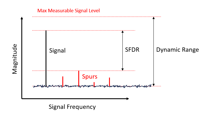
Dynamic Range. Dynamic range is the ratio of the full-scale input and the noise floor at a small or no signal input. Both quantities are usually measured separately and the different is taken as the dynamic range
Spurious free dynamic range (SFDR). SFDR measures the difference between the fundamental signal and the largest unwanted single unwanted component. It accounts for the spurs that typically comprise a spectrum.
Speed. Speed is broken down into a few different metrics:
Conversion time - The time taken for the converter to complete a single measurement - including the acquisition time of the input signal
Latency - the delay between when an input is sampled and when it is ready
In some cases, the latency can be larger than the sampling time, especially in pipelined ADCs.
Linearity. Linearity is quantified in a few ways:
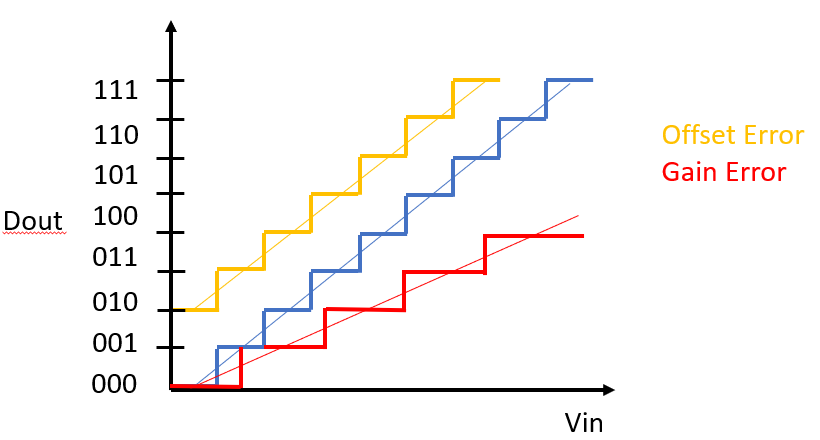
Gain Error. Gain error is the deviation of the slope of the converter output transfer function against the expected slope
Offset Error. Offset error is the DC shift in the converter transfer function from the expected one
Integral Nonlinearity error (INL). INL describes the deviation of a practical conversion curve from the ideal function
Differential Nonlinearity error (DNL). DNL describes the deviation of each step with respect to the ideal LSB size

Figure 10. INL and DNL
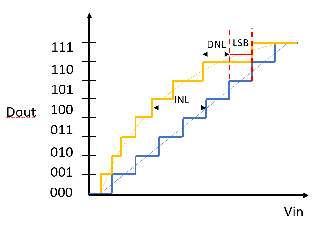
Quantization Noise and Error. Quantization error occurs in ADCs because there will always be a small offset between the digitized analog value and the actual analog value itself. This quantization noise is bounded to +- 1/2 LSB and often modelled as random white noise in the system it is in.
Important Effects
ADCs are highly sensitive to matching and noise, as well as affected by aliasing due to the sampling nature.
Aliasing. Aliasing is a broad signal processing phenomenon and occurs when the input frequency is greater than the Nyquist frequency, which is half of the sampling rate. When this happens, the frequency content above Nyquist folds back into baseband and appears as false lower-frequency content unless filtered before sampling.
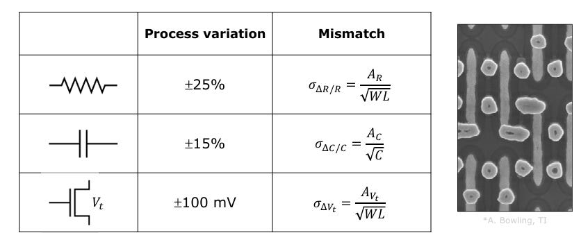
Matching. Perhaps the number one culprit of nonlinearity is the variability of components. Mismatch standard deviation generally improves roughly with the inverse square root of device area, depending on the parameter and model.
Glitches. Glitches are caused by a few things:
small voltage blips due to current switching into parasitic capacitors.
charge injection effect where the charge needed to turn the channel on/off rushes in and out,
clock feedthrough
Glitches can be reduced through careful switch timing, bottom-plate sampling, differential design, device sizing, and layout.
Calibration
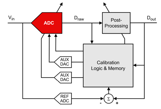
Mismatch in the DAC often necessitates calibration techniques to correct for linearity. There are two classes of calibration:
Foreground calibration - Interrupts normal operation by taking ADC out of the signal path
Background Calibration - Does not interrupt normal operation and may run continuously in the background
In each case, a quantity is injected and the raw output is observed and sent through post processing until the entire chains is linear.
Calibration can utilize reference and auxiliary ADCs/DACs to be able to “measure” the raw Dout and correct for it. Calibration can be done in the analog domain or digital domain by pre-distorting the Din to have it align to the nonlinear characteristic of the ADC.
Calibration is often necessary in high precision ADCs to correct for mismatches. However, calibration introduces additional complexity that must be properly characterized.
Conclusion
As you can see, ADCs require an in depth knowledge of analog design because they are highly sensitive to layout and noise, so designing them requires a high level of precision. Component matching is super important because it directly affects linearity. Understanding of noise sources is very important to know how each noise source affects performance.
ADC design can get especially specialized when designing for spec-defining performance in the market and advanced processes where an in-depth knowledge of ADC architectures, effects, and calibration techniques are needed. ADCs are very highly tuned to the specific application and process they are in.
I barely scratched the surface of important considerations on SAR ADCs with this primer, but I hope it helps you give you a mental framework to go more in depth in ADCs and systems they are in. Please refer to the books in the references for more information.
Also, I have a few primers on blocks that the ADC interacts with on my Substack for further reading:


References
[1] J. L. McCreary and P. R. Gray, “All-MOS charge redistribution analog-to-digital conversion techniques. I,” IEEE J. Solid-State Circuits, vol. SC-10, no. 6, pp. 371–379, Dec. 1975.
[2] T. C. Carusone, D. A. Johns, and K. W. Martin, Analog Integrated Circuit Design, 2nd ed. Hoboken, NJ, USA: Wiley, 2012.
[3] M. J. M. Pelgrom, Analog-to-Digital Conversion, 4th ed. Cham, Switzerland: Springer, 2022.